
Research Acitivities and Facilities of the Hybrid Electronic Device Lab at the INHA University, Korea
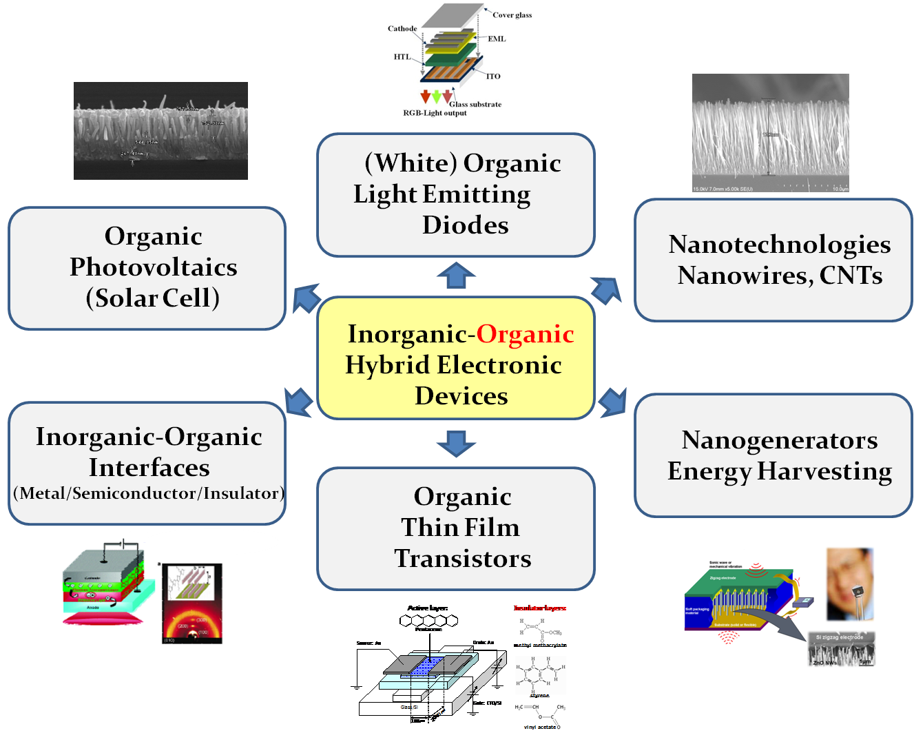
[1] Organic Electronic Devices
-Organic Light Emitting Diodes (OLEDs): vacuum evaporated organic layers for electronic display and WOLED as lighting source
-Organic Thin Film Transistors (OTFTs): based on pentacene semiconductor, plasma polymerized gate insulator
-Organic Solar Cells (OSCs): Bulk-Hetero-Juction Type Organic Thin Film Solar Cell with ZnO nanowire anode
-Flexible Organic Memories: Non-volatile Floating Gate Organic Transistor based Flexible Memory Device
[2] Synthesis of Nanowires and application to advanced Electronic Devices
-Nanowire/CNT based FETs: FET Device with active channel layer based on ZnO nanowire/CNT
-Nanowire based Generators: vertically and/or latterally structured piezoelectric power generator with ZnO nanowires
-Nanowire/CNT based FEDs
[3] Thin Film Processing and Characterization for Electronic Device Application
-Inorganic/Organic Thin Film Preparation for Hybrid Type Electronic Device Design & Fabrication
-Thin Film Surface Treatment/Thermal Treatment
-C-V, I-V, Contact Angle/Surface Energy Analysis
[4] Facilities in the Lab
-Thin Film Processing Equipments: TCP/ICP Plasma Enhance CVD for Polymer/Inorganic Thin Films; RF Plasma Surface Treatment/Polymerization System; Vacuum Thermal Evaporators for Organic & Metallic Thin Films; Spin-coater/Spary-coater.
-Nanowire Synthesis Systems: Hydrothermal Synthesis Equipments; Ultra-pure Water Production System; Precision Electronic Microblance; pH-measurement Instrument; Hot-plate with magnetic stirrer; Thermal Treatment System; Clean-Bench; Ultrasonic Cleaner.
-Device & Thin Film Characterization Systems: Probe Station; I-V/C-V Measurement Systems; Contact Angle/Surface Energy Analysis System; Micro-power Measurement System;
Last update: August 15, 2011